

IBM, today, announced their "2nm" process technology which they are calling the world's first 2nm process. Process nomenclature is quickly becoming about as standardized as the various fashion styles out there. Almost every manufacturer has its own definition of a node, with some being more lenient than others. IBM appears to have been the first to achieve a sustainable process improvement using nanosheet technology - which is far more exciting than the 2nm claim.
IBM delivers 2nm process on nanosheet technology
Typically, process shrinks offered 50% improvement for the same die area so when companies started employing exotic techniques like FinFET and got the same improvement without actually decreasing the die size - they started drifting away from the "true" value of the node size. To be clear, not a single manufacturer right now has an honest node nomenclature, but if we were to rank them in terms of strictness, Intel's naming is about twice as strict as TSMC and so on.

Intel's 7nm process for example, would be about the same as TSMC's 5nm process. TSMC's 5nm process is also not even a 50% improvement (it offers only 15% improvement over 7nm) so calling it 5nm is itself a bit of a stretch. According to IBM's claims their "2nm" technology offers a roughly 50% improvement over TSMC 7nm which would make it - at best a 3.5nm technology by even the most lenient standards of today. But I digress, there is something amazing hidden inside their message.
In a world where lithography is becoming increasingly more exotic, the race is on to find the next FinFET or manufacturing technique to continue shrinking. High NA EUV is one of these and IBM seems to have figured out another one with nanosheet technology. To me as an enthusiast, this is incredibly exciting news - far more than the 2nm marketing messaging. TSMC's lowest pitch size is 30nm and I don't expect IBM to be lower than 20nm.
It would also be interesting to see how the company manages the problems of quantum tunneling (gates no longer act as gates and electrons simply pass through transistors) and bitflipping (as transistors become smaller and smaller, cosmic rays can flip them, causing a transaction of 500 to read as 5 million for eg).
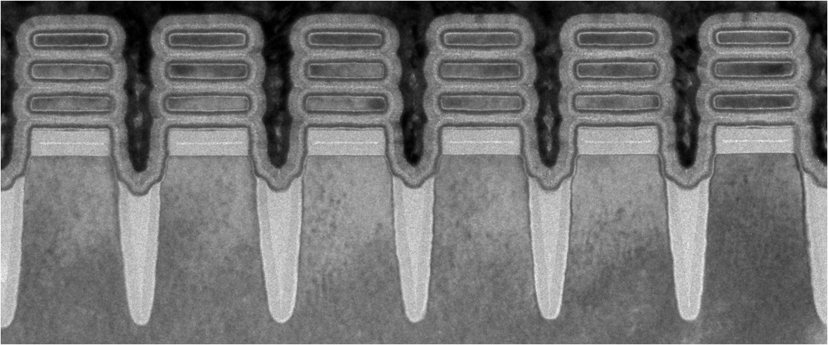
ALBANY, N.Y., May 6, 2021 — IBM (NYSE: IBM) today unveiled a breakthrough in semiconductor design and process with the development of the world’s first chip announced with 2 nanometer (nm) nanosheet technology. Semiconductors play critical roles in everything from computing, to appliances, to communication devices, transportation systems, and critical infrastructure.
Demand for increased chip performance and energy efficiency continues to rise, especially in the era of hybrid cloud, AI, and the Internet of Things. IBM’s new 2 nm chip technology helps advance the state-of-the-art in the semiconductor industry, addressing this growing demand. It is projected to achieve 45 percent higher performance, or 75 percent lower energy use, than today’s most advanced 7 nm node chipsi.
The potential benefits of these advanced 2 nm chips could include:
- Quadrupling cell phone battery life, only requiring users to charge their devices every four daysii.
- Slashing the carbon footprint of data centers, which account for one percent of global energy useiii. Changing all of their servers to 2 nm-based processors could potentially reduce that number significantly.
- Drastically speeding up a laptop’s functions, ranging from quicker processing in applications, to assisting in language translation more easily, to faster internet access.
- Contributing to faster object detection and reaction time in autonomous vehicles like self-driving cars.
“The IBM innovation reflected in this new 2 nm chip is essential to the entire semiconductor and IT industry,” said Darío Gil, SVP and Director of IBM Research. “It is the product of IBM’s approach of taking on hard tech challenges and a demonstration of how breakthroughs can result from sustained investments and a collaborative R&D ecosystem approach.”
IBM at the forefront of semiconductor innovation
This latest breakthrough builds on decades of IBM leadership in semiconductor innovation. The company’s semiconductor development efforts are based at its research lab located at the Albany Nanotech Complex in Albany, NY, where IBM scientists work in close collaboration with public and private sector partners to push the boundaries of logic scaling and semiconductor capabilities.This collaborative approach to innovation makes IBM Research Albany a world-leading ecosystem for semiconductor research and creates a strong innovation pipeline, helping to address manufacturing demands and accelerate the growth of the global chip industry.
IBM’s legacy of semiconductor breakthroughs also includes the first implementation of 7 nm and 5 nm process technologies, single cell DRAM, the Dennard Scaling Laws, chemically amplified photoresists, copper interconnect wiring, Silicon on Insulator technology, multi core microprocessors, High-k gate dielectrics, embedded DRAM, and 3D chip stacking. IBM’s first commercialized offering including IBM Research 7 nm advancements will debut later this year in IBM POWER10-based IBM Power Systems.
50 billion transistors on a fingernail-sized chip
Increasing the number of transistors per chip can make them smaller, faster, more reliable, and more efficient. The 2 nm design demonstrates the advanced scaling of semiconductors using IBM’s nanosheet technology. Its architecture is an industry first. Developed less than four years after IBM announced its milestone 5 nm design, this latest breakthrough will allow the 2 nm chip to fit up to 50 billion transistors on a chip the size of a fingernail.More transistors on a chip also means processor designers have more options to infuse core-level innovations to improve capabilities for leading edge workloads like AI and cloud computing, as well as new pathways for hardware-enforced security and encryption. IBM is already implementing other innovative core-level enhancements in the latest generations of IBM hardware, like IBM POWER10 and IBM z15.
The post IBM Unveils The World’s First ‘2nm’ Technology With Nanosheets – But Don’t Let That 2nm Tag Fool You by Usman Pirzada appeared first on Wccftech.
source https://wccftech.com/ibm-unveils-the-worlds-first-2nm-technology-with-nanosheets-but-dont-let-that-2nm-tag-fool-you/